Table of Contents
ToggleIn 1839, physicist Edmond Becquerel discovered the photovoltaic effect while experimenting with a cell made of metal electrodes in a conducting solution. He noted that the cell generated more electricity when exposed to light.
Albert Einstein had to bring attention to solar energy and its potential. In 1905, he published a paper on the photoelectric effect and how light carries energy. This generated more awareness and acceptance for solar power on a broader scale.
The big leap toward solar cells like the ones used in panels today came from the work of Bell Labs in 1954. Three scientists there, Daryl Chapin, Calvin Fuller, and Gerald Pearson, created a more practical solar cell using silicon. Advantages to silicon are better efficiency and its wide availability as a natural resource.
In 2020, solar cell efficiency of perovskite solar cells has risen from 3.8% in 2009 to 25.2%. Scientists have proven that adding an organic-based ionic solid into perovskites can substantially improve solar cell performance and stability.
What are solar cells?
Solar cells do not utilise chemical reactions or need fuel to generate electric power.
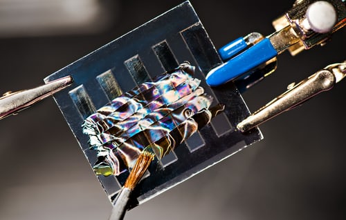
Also known as the photovoltaic cell, the solar cell refers to any device that directly converts the energy of light into electrical energy through the photovoltaic effect. They are often bundled together to make larger units known as solar panels.
Most solar cells are made from silicon due to its increased efficiency and lower cost. The materials vary from amorphous (noncrystalline) to polycrystalline and crystalline (single crystal) silicon types.
Solar cells do not require fuel to produce electric power, and unlike electric generators, they don’t have any moving parts.
Solar cells can be arranged into broad groupings called arrays. These arrays, composed of many thousands of individual cells, can function as central electric power stations, converting sunlight into electrical energy for distribution to industrial, commercial, and residential users.
Types of photovoltaic solar cells
Photovoltaic cells or PV cells can be produced in many different ways and from other materials. Despite the difference, they all perform the same task of collecting solar energy and turning it into valuable electricity.
The most common material for the solar panel is silicon which has semiconducting properties. There are two major types of photovoltaic cell materials used – crystalline silicon and thin film deposits. These two types are different in terms of light absorption efficiency, energy conversion efficiency, manufacturing technology, and cost of production.
-
Monocrystalline Silicon Cell
It is a kind of photovoltaic cell material made from a single-crystal silicon structure, which is uniform in shape because the whole structure is grown from the same crystal.
-
Polycrystalline Silicon
It is also known as multi-crystalline silicon, and polycrystalline silicon is made by merely casting a cube-shaped ingot from molten silicon, then sawn and packaged similarly to monocrystalline cells.
The silicon molecular structure consists of several smaller groups or grains of crystals, which introduce boundaries.
-
Thin Film Solar Cell
It is another type of photovoltaic cell initially developed for space applications with a better power-to-size and weight ratio. Thin film photovoltaics are produced by printing or spraying a thin semiconductor layer of PV material onto a glass, metal, or plastic foil substrate.
How are solar cells made?
Stage One: Purifying the silicon
The silicon dioxide is put in an electric arc furnace. Then, a carbon arc is used to release the oxygen.
The products resulting from it are carbon dioxide and molten silicon. This will produce silicon that has 1% impurity. However, it is not pure enough for solar cells.
The silicon, currently at 99% purity, is refined even more using the floating zone technique. A rod of impure silicon is several times passed through a heated zone in the same way.
The procedure drags impurities towards one end with each pass. Eventually, the silicon will be considered pure, and the impure end will be separated.
Stage Two: Making a single crystal silicon
Solar cells are made from silicon boules. These are polycrystalline structures that have the atomic composition of a single crystal.
The most commonly used technique for the production of the boule is known as the Czochralski method. During this method, a seed crystal of silicon is immersed into melted polycrystalline silicon.
As the seed crystal is removed, it is turned, which means the silicon’s boule forms a cylindrical ingot. The ingot is pure, as all impurities are gone in the liquid.
Stage Three: Making silicon wafers
Silicon wafers from the boule are sliced separately using a circular saw. The inner diameter cuts into the rod. A diamond saw is the best for slicing and producing a cut as wide as the wafer.
Around half of the silicon is lost from the boule to the finished circular wafer, though more can be lost if it is cut in rectangular or hexagonal.
These shapes are sometimes used in solar cells because they fit together nicely, using all of the space on the solar cell’s surface.
The wafers are then polished to remove any saw marks, although some manufacturers have chosen to leave the marks because they found that rougher cells may absorb light more effectively.
Stage Four: Doping
The most recent form of doping silicon with phosphorous is using a small particle accelerator to ‘shoot’ the phosphorous ions into the ingot.
By regulating the speed of the ions, it becomes possible to control the extent of diffusion.
However, this new process has not been entirely accepted. The traditional method tends to include the introduction of a small amount of boron during the previous stage.
Stage Five: Placing electrical contacts
Electrical contacts are used to connect one solar cell to the other.
The contact needs to be extremely thin to not block any sunlight from being limited by the cell.
Through a photoresistor deposited on the exposed part of cells that have been partly coated with wax, metals like palladium or copper are vacuum evaporated.
After contacts have been put in place, thin strips are placed between the cells. The most commonly used strips are tin-coated copper.
Stage Six: The anti-reflective coating
Pure silicon is often shiny to enable it to reflect up to 35% of the sunlight. An anti-reflective coating is put onto the silicon wafer to reduce the amount of sunlight that is lost.
Titanium dioxide and silicon oxide are the most commonly used coatings. The material used for the coating is either heated until the molecules boil off or the material undergoes sputtering.
High voltage will knock molecules off the material, deposit them onto the silicon, and then transfer it onto the opposite electrode’s silicon.
Stage Seven: Encapsulating the cell
The now finished solar cells are encapsulated. This means that they are sealed into silicon rubber or ethylene-vinyl acetate.
The encapsulated solar cells are then placed into an aluminium frame with a Mylar or Tedlar back-sheet and a glass or plastic cover.
Why is silicon used in solar cells?
Silicon is the most popular semiconductor material used in solar cells, representing nearly 95% of the modules sold today. It is also the second most ample material on Earth (after oxygen).
In the old days, silicon solar cells used to be rather expensive, as very high-quality silicon was required to make them. Also, the procedure of purification of silicon before intervening with gallium and arsenic atoms used to be time-consuming and costly.
Fortunately, the evolution of technology soon allowed the use of cheaper and lower quality silicon resulting in silicon solar cells being more affordable, especially with government subsidies.
Solar cells made out of silicon provide high efficiency, low cost, and long endurance. Modules are expected to last for 25 years or more, still producing more than 80% of their original power after this time.
How do solar cells work?
The photovoltaic effect is a process that generates a voltage or electric current in a photovoltaic cell when it is exposed to sunlight.
This effect makes solar panels useful, as it is how the cells within the panel convert sunlight to electrical energy.
In 1939, Edmond Becquerel first discovered the photovoltaic effect. When doing experiments involving wet cells, he noted that the cell’s voltage increased when its silver plates were exposed to the sunlight.
The effect occurs in solar cells. These solar cells are composed of two types of semiconductors, called p-type and n-type silicon. The p-type silicon is created by adding atoms like boron or gallium with one less electron in their outer energy level than silicon.
The n-type silicon is made by combining atoms that have an extra electron in the outer level than silicon.
Phosphorus has five electrons on its outer energy level. It bonds with its silicon neighbour atoms, but one electron is not required in bonding. Instead, it can move freely inside the silicon structure.
A solar cell consists of a layer of p-type silicon placed next to a layer of n-type silicon. In the n-type layer, there is an abundance of electrons, and in the p-type layer, there is an excess of positively charged holes.
Near the intersection of the two layers, the electrons on one side of the junction (n-type layer) flow into the holes on the other side of the intersection (p-type layer). This produces an area around the intersection, called the depletion zone, in which the electrons fill the holes.
When all the holes are occupied with electrons in the depletion zone, the depletion zone’s p-type side (where holes were initially present) now contains negatively charged ions. The n-type side of the depletion zone (where electrons were present) now contains positively charged ions.
The presence of these oppositely charged ions creates an internal electric field that prevents electrons in the n-type layer from filling holes in the p-type layer.
When sunlight strikes a solar cell, electrons in the silicon are ejected, which results in the formation of “holes”. If this happens in the electric field, the field will move electrons to the n-type layer and holes to the p-type layer.
Suppose the n-type and p-type layers are connected with a metallic wire. In that case, the electrons will move from the n-type layer to the p-type layer by passing the depletion zone and then go through the external wire of the n-type layer, creating a flow of electricity.
How do grid connections work with solar panels?
When a homeowner chooses to add solar panels to their home, often, they will decide to be grid-connected. This means that the house will get electricity both from its solar panels and the electric grid.
This is significant because solar energy is intermittent. It stops when the sun goes down. So, the grid-connected solar home will automatically use electricity from the grid to meet its electricity needs. This process happens automatically.
In the other case, when solar panels produce more electricity than what the home needs, it will send the extra electricity into the grid. That solar electricity will then be used by the neighbourhood. No electricity gets wasted.
Solar cell efficiency
It is essential to understand that the efficiency of an individual solar cell does not equate to solar panels’ efficiency. While solar panel efficiency is generally around 15-20%, solar cell efficiency can reach 42% in some cases.
However, unless otherwise stated, the performance of solar cells is measured under laboratory conditions. Therefore, although 42% is an impressive performance, laboratory conditions are different from real life, which does not apply to residential users.
Energy loss in a Solar Cell
When sunlight is received in a solar cell, negatively charged electrons and positively charged holes are created, which drives electrical current generating power.
The absorbed light generates electrons and holes with a series of energies. Those with greater energy, called “hot” electrons and holes, tend to lose energy in the form of heat before it can be converted into an electrical current.
Conversion of hot carriers’ energy into heat is the main source of energy loss in solar cells. These losses are fundamental to many energy conversion processes and occur in most electronic energy conversion devices.
Further, they occur at ultrafast speeds, typically less than one picosecond. Due to the sub-picosecond time scale and complex physics involved, hot carriers’ characterisation has long been a challenge even for the simplest materials.
Current Updates
24 Nov 2020 – A team of researchers at the Hebrew University of Jerusalem has developed a technique for producing recyclable perovskite used in solar cells.
The new technique by the team involves using screen-printed, three-layered all-nanoparticle networks as rigid frameworks for building cells based on perovskites.
Such frameworks allow the perovskites to strain in a way that leads to photoactive networks.
Testing of the technique showed it to be equal in efficiency to perovskite cells that do not allow easy recycling.
The team also tested their technique by allowing one of the cells to run long enough to degrade and then recycled the perovskite material after doing so. The cell was found to be just as efficient as new cells.
23 Nov 2020 – Solar panels used to always be about harvesting energy from sunlight to generate power or electricity.
But scientists have now developed new materials for solar cells that can take energy from light bulbs found inside our homes and offices and use it to power everyday smart devices.
The idea with an indoor solar cell is that by making them, they can last for the entire lifetime of the device itself.
As long as there’s some ambient lighting available, then it can convert that energy to power the device, so there is no need to keep on replacing the power source.
16 Nov 2020 – India’s government has agreed on a financing package that includes US$603 million of investment over five years to support the domestic development of high-efficiency PV modules.
Solar modules form one of ten “key sectors” included in a production-linked incentive (PLI) scheme that has been green-lighted by India’s cabinet in a move to help make domestic manufacturers globally competitive, create economies of scale and boost exports.
The government said that ACC battery manufacturing represents “one of the largest economic opportunities of the 21st century” for sectors such as renewable energy, electric vehicles and consumer electronics.
27 Oct 2020 – A new study says, designing solar panels in checkerboard lines increases their ability to absorb light by 125%.
Researchers say the breakthrough could lead to the production of thinner, lighter and more flexible solar panels that could be used to power more homes and be used in a wider range of products.
The study investigated how different surface designs impacted the absorption of sunlight in solar cells, which, when put together form solar panels.
Scientists found that the checkerboard design improved diffraction, which enhanced the probability of light being absorbed that is then used to create electricity.
Conclusion
Edmond Becquerel first observed the photovoltaic effect when doing experiments with wet cells. He saw that its voltage increased when its silver plates were exposed to the sunlight.
The effect occurs in solar cells. A solar cell is a sandwich of n-type silicon and p-type silicon. It produces electricity by using sunlight to make electrons jump across the junction between the different silicon.